MEMS encapsulation materials shall balance low‑stress performance, environmental protection, media resistance and precision dispensing capability. For pressure sensors, automotive sensors and industrial MEMS devices, soft gel can be adopted for local protection when rigid potting materials may impose mechanical stress on sensitive structures. ELAPLUS FSGEL 3200C is a one‑component thixotropic fluorosilicone gel. It delivers flexible coating for MEMS chips, solder joints and lead areas, and is applicable for sensor encapsulation exposed to harsh media such as oil, fuel, solvents and moisture.
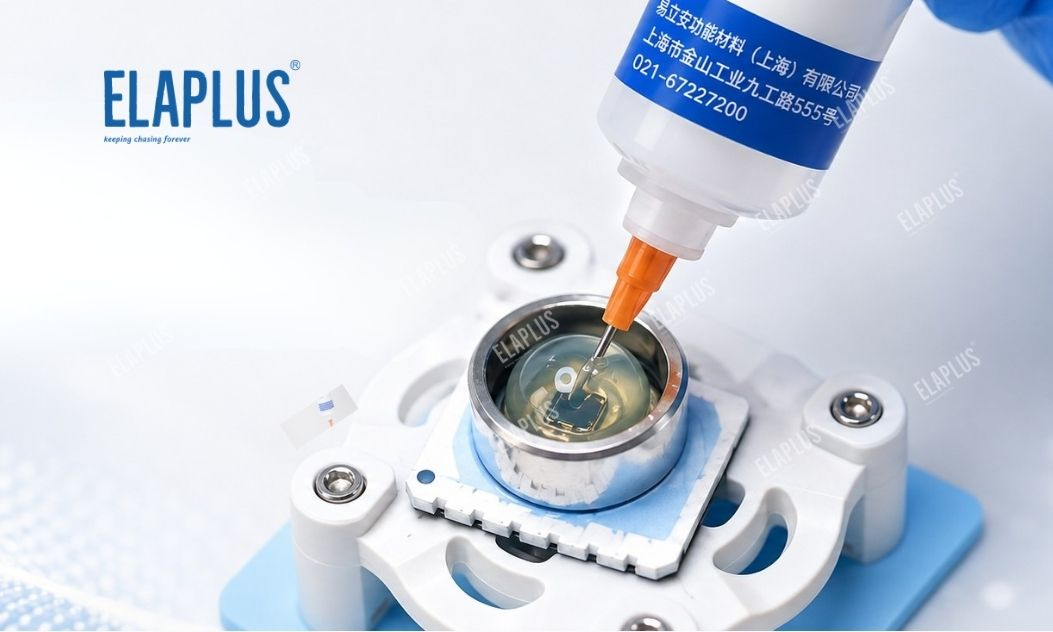
This marks one major difference between MEMS encapsulation and ordinary PCB potting: MEMS encapsulation is not merely “sealing the chip”. It aims to provide protection while minimizing material‑induced interference to sensitive structures.
Why Low‑stress Materials Are Required for MEMS Encapsulation
MEMS stands for Micro‑Electro‑Mechanical System. Such devices integrate micro‑mechanical structures, sensing elements, electrodes, solder joints or gold wires to detect external signals such as pressure, temperature and acceleration. Therefore, MEMS chips are vulnerable not only to moisture and corrosion, but also to mechanical stress originating from encapsulation materials.
Taking MEMS pressure sensors as an example, high‑modulus encapsulants or materials with significant shrinkage and expansion during curing and thermal cycling may alter the original stress state of sensitive structures.
Potential consequences include:
‑ Zero‑point drift of chips
‑ Deviation of output signals
‑ Shift in sensitivity
‑Long‑term stress applied to gold wires and solder joints
‑ Reliability failures after thermal cycling
Accordingly, for certain MEMS applications, encapsulation material evaluation shall not focus solely on hardness or bonding strength. Of greater importance is whether the material can offer environmental protection while mitigating mechanical disturbance to sensitive structures.
What Is FSGEL 3200C?
FSGEL 3200C is a one‑component thixotropic fluorosilicone gel for flexible protection of sensitive electronic components and sensors. Unlike conventional high‑hardness potting materials, it remains soft after curing and forms cushioning protective layers around chips, solder joints and leads.
Three core advantages for MEMS encapsulation: low‑stress performance, precision dispensing and harsh‑media compatibility
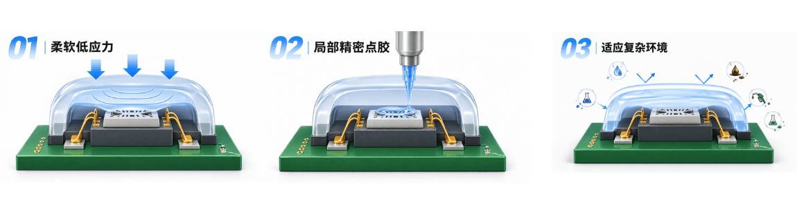
01 Soft & Low‑stress: Reduce Material Interference on MEMS Chips
Internal structures of MEMS chips are extremely delicate. In many cases, engineers do not want the chip to be rigidly locked by encapsulant. Instead, the material shall coat the chip while maintaining sufficient flexibility.
After curing, FSGEL 3200C forms soft gel covering MEMS chips, solder joints and surrounding leads. This flexible coating helps cushion:
‑ Temperature variation
‑ Thermal expansion and contraction
‑ Vibration
‑ Mechanical shock
‑ Deformation mismatch among dissimilar materials
For stress‑sensitive MEMS devices such as pressure, force and acceleration sensors, reducing encapsulation‑induced stress is often more critical than pursuing high material hardness.
02 Local Precision Dispensing: Suited for Miniature MEMS Encapsulation
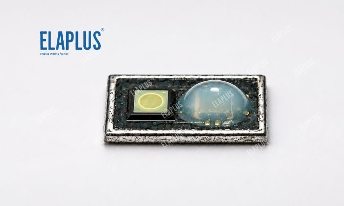
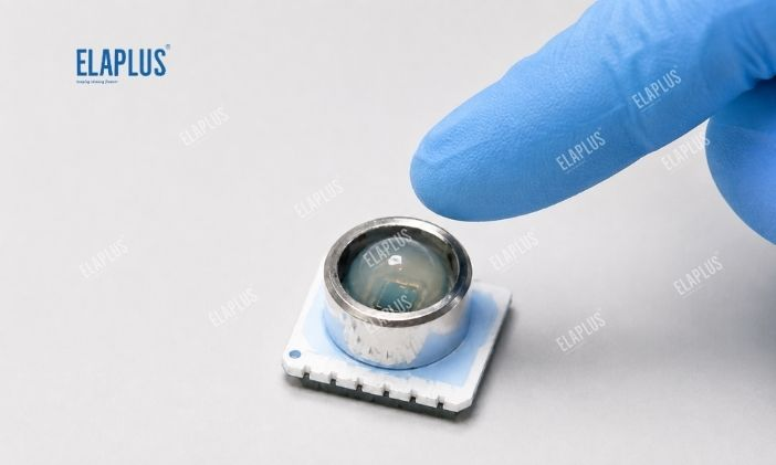
MEMS sensors are compact in size. Full‑cavity potting is unnecessary for many products. Local dispensing protection targeting only MEMS chips and key sensitive zones is the common practice.
As a one‑component material, FSGEL 3200C can be applied onto designated chip areas via needles or precision dispensing equipment. Typical workflow for MEMS pressure‑sensor encapsulation is shown below: Step 1: Locate the MEMS chip. Move dispensing needle above the chip according to sensor geometry.
Step 2: Quantitative dispensing. Control material output to gradually cover chip surface with gel.
Step 3: Cover solder joints and lead zones. Extend gel coverage over sensitive areas requiring protection as per structural requirements.
Step 4: Form continuous flexible protective layer. A stable gel protective structure is built on top of the MEMS chip.
Local dispensing fits miniature sensors well and cuts redundant material consumption.
Why Fluorosilicone Gel for MEMS Encapsulation?
MEMS devices are exposed to more than moisture. In automotive, industrial control and pressure‑measurement scenarios, sensors may encounter:
‑ Oil
‑ Fuel
‑ Oil vapors
‑ Solvents
‑ Chemical media
‑ Repeated thermal cycling
‑ Long‑term vibration
Thus encapsulation materials for these applications require not only low‑stress property but also compatibility with complex media environments. Fluorosilicone systems combine flexible protection and resistance to aggressive media. For automotive and industrial pressure sensors, material selection cannot rely merely on waterproof performance; validation against actual contact media is mandatory.
Problems Solved by FSGEL 3200C in MEMS Encapsulation
Based on practical MEMS encapsulation requirements, FSGEL 3200C addresses the following challenges:
- Mitigate mechanical stress Soft gel coats MEMS chips and lowers risks imposed by rigid encapsulants on sensitive structures.
- Protect gold wires and solder joints Fine bonding wires and solder joints around MEMS chips gain cushioning protection under gel coverage.
- Reduce impacts from moisture and contaminants Continuous gel barriers isolate external moisture and pollutants from chip surfaces.
- Resist oil, fuel and solvent environments Critical for long‑term reliability of automotive and industrial sensors exposed to oils, fuels and solvents.
- Enable local precision encapsulation Quantified dispensing only on targeted chip zones for compact MEMS components instead of full‑board potting.
MEMS Pressure‑sensor Encapsulation Case
A MEMS pressure sensor normally features a central sensing chip, surrounded by pads, electrodes, leads and signal‑processing circuits. Direct exposure of these zones may lead to degradation caused by moisture, oil, temperature swing and mechanical vibration over service life.
In such structures, FSGEL 3200C can be dispensed precisely onto MEMS chip regions. Gel spreads over the chip and adjacent critical zones to build a soft, continuous local protective layer. Compared with full rigid encapsulation, this design philosophy prioritizes protecting MEMS rather than constraining MEMS, which is a key principle for material selection of sensors with functional sensitive structures.
Key Considerations for MEMS Encapsulation Dispensing
Even with proper material selection, process control remains vital.
- More gel does not equal better protection Gel height and coverage shall be strictly controlled for MEMS encapsulation. Insufficient material fails to form intact barriers; excessive gel may intrude forbidden zones. Determine dispensing volume according to chip dimension, cavity geometry and target coverage area.
- Pay attention to pressure ports and functional zones MEMS chip architectures vary greatly. Some pressure sensors contain pressure channels, vent holes or sensitive diaphragms. Confirm whether these features allow gel coverage according to device specifications. Do not assume all areas of MEMS chips can be potted.
- Control bubbles during dispensing Bubbles may result in discontinuous coverage for miniature sensor encapsulation. Process parameters to be optimized: needle gauge, dispensing pressure, flow rate, dispensing gap, material dosage and material storage condition.
- Mandatory reliability validation MEMS sensors operate under diverse conditions. Automotive pressure sensors, industrial sensors and consumer‑grade electronic sensors endure different temperature, media and vibration loads. Final material suitability shall be verified on end‑products via media compatibility, thermal cycling, aging, vibration and electrical‑performance tests.
Recommended Application Scenarios for FSGEL 3200C
- MEMS pressure sensors: Local protection for sensing chips and surrounding structures.
- Automotive sensors: Encapsulation for sensors exposed to oil, fuel, moisture and complex environments.
- Industrial sensors: Protection for pressure, temperature and other sensitive electronic structures.
- Micro‑electronic devices: Flexible low‑stress coating for precision electronic components.
- Partial chip protection: Sensitive zones unsuitable for full potting with high‑hardness materials.
How to Select MEMS Encapsulation Materials
Evaluate the following criteria for local‑protection MEMS applications:
| Selection Factor | Key Concerns |
|---|---|
| Material softness | Whether obvious mechanical stress is exerted on sensitive chips |
| Gel morphology | Ability to stably cover chips and solder joints |
| Dispensing performance | Suitability for micro‑volume, quantitative and local dispensing |
| Media compatibility | Exposure to oil, fuel, solvents or chemical agents |
| Environmental reliability | Resistance to thermal cycling, vibration and humidity‑heat conditions |
| Chip architecture | Presence of gel‑prohibited functional zones |
| Process requirements | Compatibility with dispensing speed, dosage and needle specifications |
There is no universal “best” MEMS encapsulation material. The core lies in matching material properties with sensor structure and service environment.
FAQ
Q: Can FSGEL 3200C be used for MEMS encapsulation? A: It can be evaluated as local flexible‑protection material for MEMS chips, especially for sensors requiring low‑stress performance, precision dispensing and harsh‑media resistance. Final validation against specific chip structures and reliability requirements is necessary.
Q: Why are rigid potting compounds not always suitable for MEMS chips? A: Some MEMS devices are highly stress‑sensitive. High‑modulus or high‑shrinkage materials may alter chip stress status. Suitability shall be judged case‑by‑case according to device type.
Q: Can MEMS pressure sensors be fully filled with adhesive? A: A one‑size‑fits‑all approach is not recommended. Confirm whether pressure ports, sensitive diaphragms, channels and functional zones allow gel coverage before determining dispensing position and dosage.
Q: What is the difference between fluorosilicone gel and ordinary silicone gel? A: Both deliver flexible protection. Fluorosilicone grades excel in harsh‑media environments such as oil, fuel and certain chemical agents. Actual compatibility testing is still required.
Q: Is waterproofing the top priority for MEMS encapsulation? A: No. MEMS encapsulation requires comprehensive consideration of mechanical stress, chemical media, moisture, thermal cycling, vibration and device geometry. Waterproof performance alone cannot define material suitability.
Conclusion
Driven by automotive electronics, industrial sensors and smart devices, MEMS devices are trending toward miniaturization, higher sensitivity and deployment in harsher environments. The core objective of MEMS encapsulation is shifting from simply “sealing the chip” to “achieving long‑term reliable protection with minimal interference to sensitive structures”.
ELAPLUS FSGEL 3200C, one‑component thixotropic fluorosilicone gel, provides local flexible protection for MEMS chips, solder joints and leads. It is available for material evaluation for sensors operating under complex environments involving oil, fuel and solvents.
ELAPLUS Original Manufacturer|Selection Support|Free Samples Available info@elaplus.cc