Packaging materials for MEMS pressure sensors must satisfy multiple requirements simultaneously: low stress, moisture resistance, electrical insulation, protection for gold wires and solder joints, and medium resistance in practical environments. Since MEMS operates relying on tiny mechanical structures, excessive material modulus, curing shrinkage and thermal expansion stress may cause zero drift or signal variation. ELAPLUS FSGEL 3200C is a one-component thixotropic fluorosilicone gel, which is suitable for flexible, low-stress and medium-resistant protection of MEMS chips, gold wires and sensitive electronic areas. It is NOT designed for primary structural bonding of magnetic steel, housings and other load-bearing structures.
When packaging sensitive chips such as MEMS pressure sensors and micro-pressure sensors, the core principle for material selection is not “the harder and firmer, the better”. Instead, materials shall provide moisture-proof, anti-corrosion, oil/gas and chemical medium resistance, gold wire and solder joint protection, while minimizing mechanical stress exerted on chips by packaging materials.
That is why for certain MEMS sensor protection scenarios, soft, low-stress fluorosilicone gel is preferable compared with traditional high-modulus rigid potting materials.
Take ELAPLUS FSGEL 3200C one-component thixotropic fluorosilicone gel as an example. Its main function in application is not to fix the housing structure, but to form a flexible protective layer over MEMS chips, gold wires, solder joints and sensitive electronic regions.
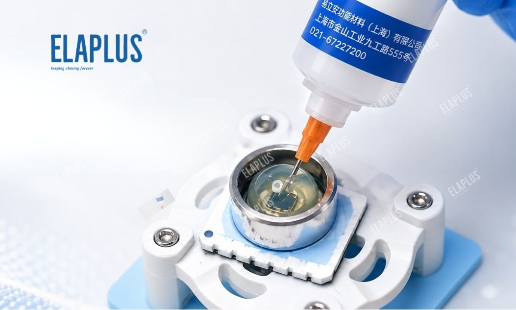
In short: The real challenge of MEMS packaging is not merely “covering the chip”, but protecting it without interfering with its sensing function.
I. Why Are MEMS Sensors More “Vulnerable to Adhesives” Than Ordinary PCBs?
For ordinary PCB potting, we usually expect materials to fix components, resist moisture and water, provide insulation and resist vibration. However, MEMS devices have one special requirement: They work based on micro-deformation.
MEMS stands for Micro-Electro-Mechanical Systems. Take MEMS pressure sensors as an example. Pressure acts on the internal sensitive structure of the chip, converting tiny mechanical changes into electrical signals.
Here comes a seemingly contradictory issue: External vibration shall not affect it; The packaging material itself shall not affect it either.
If the packaging material is too hard, features large curing shrinkage, or imposes strong mechanical constraint on the chip during temperature fluctuation, the packaging material itself will become an extra “force source”.
II. What Risks Does MEMS Packaging Face?
| MEMS Packaging Risk | Possible Impact | Material Requirements |
|---|---|---|
| Oil, fuel vapor and chemical media | Corrosion of chips and soldering zones | Medium resistance and anti-corrosion |
| Water vapor ingress | Electric leakage, corrosion and abnormal performance | Moisture resistance and insulation |
| Thermal expansion and contraction | Additional stress on chips | Low modulus and flexibility |
| Micro-vibration of gold wires | Fatigue failure of gold wires/solder joints | Flexible buffering |
| Curing shrinkage | Zero-point shift | Low stress |
| Temperature cycling | Zero drift and signal variation | Long-term stability |
| Rigid material directly restraining chip core | Impaired sensitivity | Reduction of mechanical interference |
Therefore, when evaluating materials for MEMS, we should not only check: Hardness and bonding strength. We must also verify: Whether the sensor remains accurate after the material is applied.
III. How Can Rigid Potting Materials Affect MEMS?
Assume a pressure chip is initially in free state, with a stable zero point when external pressure equals zero. When a layer of high-modulus resin is applied around the chip, shrinkage occurs during material curing and may generate tensile, compressive or bending constraints on the chip. Even without new external pressure, the stress state of the sensitive structure has changed.
The final phenomenon may be: normal zero point before potting → zero shift after curing.
At high temperatures: The thermal expansion coefficients of gel, metal substrate, ceramics and chips do not match completely. New stress will emerge again. This is one of the key reasons that MEMS packaging needs to focus on verifying zero drift and thermal drift.
IV. What Is the Value of Low-Stress Gel?
The biggest feature of gel-type materials is not “no strength”. They remain soft after curing.
For sensitive electronic devices, this means the material can realize environmental isolation while reducing rigid constraints.
To make it easier to understand: ordinary rigid potting is like “fixing the component inside a hard shell”. Flexible gel is like “adding a soft protective layer for sensitive devices”. These two solve different problems.
V. What Problems Can FSGEL 3200C Solve in MEMS Packaging?
ELAPLUS FSGEL 3200C One-component Thixotropic Fluorosilicone Gel
Its core advantages in MEMS applications fall into three categories:
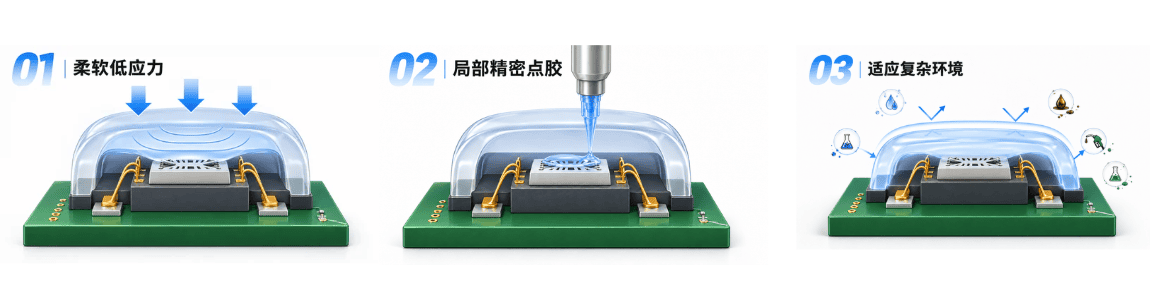
01 Soft & Low Stress
It forms a soft, self-buffering gel protective layer after curing. It can cover: MEMS chips; Gold wires; Solder joints; Local electronic components.
It can buffer mechanical disturbances caused by temperature change, vibration and other factors. The core goal is NOT “extremely firm fixation”. Instead: “Minimize extra stress imposed on sensitive structures.”
02 Local Precision Dispensing
FSGEL 3200C adopts a one-component system for local dispensing on sensitive areas. Compared with fully potting the entire sensor cavity with rigid material, this method is suitable for: Targeted protection only where needed.
For instance, when the MEMS chip is located at the center of a PCB or ceramic substrate, the material can be applied selectively to cover: Chips, gold wires and soldering zones. It provides local environmental protection and avoids unnecessary bulk material coverage.
03 Protection for Harsh Media Environments
Automotive and industrial MEMS do not always work in dry and clean conditions. They may be exposed to: Oil; Fuel vapor; Moisture; Partial chemical media; Temperature variation environments.
As a fluorosilicone gel, one of the key strengths of FSGEL 3200C is medium resistance, moisture-proof, anti-corrosion and electrical insulation protection. It is especially worth evaluating for automotive pressure sensors, industrial pressure sensors and other devices operating in harsh environments.
VI. Why We Cannot Simply Treat Ordinary Silicone and Fluorosilicone Gel as “Both Soft Gels”
This is a common confusion in material selection. Low stress is only the first consideration. The operating environment must also be assessed.
| Selection Item | Ordinary Flexible Protective Material | Fluorosilicone Gel |
|---|---|---|
| Low stress | Assessable | Core advantage |
| Moisture resistance | Assessable | Assessable |
| Electrical insulation | Assessable | Assessable |
| General electronic environment | Suitable | Usable upon necessity check |
| Oil/gas & complex media | Special verification required | Highly recommended for evaluation |
| MEMS sensitive areas | Depends on formulation | FSGEL 3200C for priority evaluation |
| Primary structural bonding | Depends on specific structural adhesive | Not for primary use |
Special note on the last point: The core task of FSGEL 3200C is sensitive device protection, NOT primary structural bonding of the whole sensor.
If your requirement is: Bonding aluminum housing and plastic housing, load-bearing housing, fixing metal structures, structural adhesives or sealants shall be selected instead.
VII. Why “Thicker Gel Does Not Equal Safer” for MEMS Packaging?
This is a typical industry misconception. Many people think: Gel is soft, so more gel means better protection. This is not necessarily true.
Even soft gel, when applied in larger quantity, may change: mass around the chip; heat transfer; structural coupling; medium transmission path; subsequent rework process.
Especially since MEMS chips are tiny. What is really needed: Reasonable coverage of sensitive regions. Not excessive bulk gel just for “full filling”.
VIII. Pre-potting & Post-potting Verification for MEMS Pressure Sensors
It is recommended to build the following test dataset.
| Verification Stage | Key Records |
|---|---|
| Before dispensing | Initial zero point |
| Right after dispensing | Instant output variation |
| Fully cured | Offset induced by curing |
| High temperature | High-temperature zero drift |
| Low temperature | Low-temperature zero drift |
| After thermal cycling | Whether it can return to the initial state |
| After medium aging | Zero point, sensitivity |
| After vibration test | Gold wires, solder joints and signal |
Reason for these tests: Material suitability cannot be judged only by the gel itself. The final judgment depends on sensor performance.
IX. Troubleshooting Checklist for Zero Drift after MEMS Potting
| Phenomenon | Highly Suspected Cause |
|---|---|
| Variation immediately after dispensing | Gel weight / structural contact |
| Variation appears only after curing | Curing stress |
| Obvious drift at high temperature | CTE and thermal stress |
| Recovers after cooling | Reversible thermal stress |
| Does NOT recover after cooling | Residual mechanical stress |
| Greater drift with thicker gel | Potting area / coating thickness |
| Large batch-to-batch difference | Dispensing volume, curing process |
| Drift after oil aging | Medium compatibility |
This table is practical for on-site engineering use.
If zero drift occurs only after curing, priority should be given to packaging materials and curing process. If drift appears only under high temperature, thermal expansion matching needs further investigation.
X. Industry Pitfalls|5 Common Misconceptions in MEMS Packaging
Pitfall 1: Harder protective material means higher reliability. It may hold for ordinary structural parts, but high rigidity will increase mechanical constraints for sensitive MEMS.
Pitfall 2: Passing IP waterproof test means the packaging solution is qualified. MEMS requires extra verification for zero point, thermal drift and sensitivity. Waterproof performance and measurement accuracy are two separate dimensions.
Pitfall 3: Directly apply ordinary electronic potting experience to MEMS. MEMS chips have completely different stress sensitivity compared with common resistors and capacitors.
Pitfall 4: More adhesive provides better protection. Excessive potting does not bring extra effective protection; it may alter structural behavior instead.
Pitfall 5: Using low-stress material removes the need for functional tests. This is the most dangerous misunderstanding. Low stress is the material design direction, not an absolute guarantee of zero impact in all structures. Verification on real chips is mandatory.
XI. Suitable Application Scenarios for FSGEL 3200C
The following scenarios are recommended for priority evaluation:
- MEMS pressure sensors Especially for flexible local protection of sensitive chips, gold wires and solder joints.
- Automotive pressure / oil pressure sensors Requiring low stress and resistance to oil and gas media.
- Industrial pressure sensors Long-term exposure to moisture, temperature fluctuation and industrial environments.
- Precision micro-pressure devices Highly sensitive to mechanical disturbance and requiring minimized packaging impact.
- Sensitive electronic devices with medium resistance requirements Needing both flexibility and environmental isolation.
XII. Scenarios Where FSGEL 3200C Is NOT Recommended Directly
This part is critical; this product is not universal.
| Scenario | Recommended? |
|---|---|
| Flexible protection of MEMS chip | ✓ Priority evaluation |
| Gold wire / solder joint protection | ✓ |
| Protection of sensitive electronics in oil/gas environment | ✓ |
| Primary structural bonding of sensor housing | × |
| High-strength bonding of magnetic steel | × |
| Load-bearing metal structures | × |
| Large-volume high-hardness mechanical fixation | × |
| TIM between MOSFET and heat sink | × |
Select adhesives based on working conditions, not just stacking parameters.
XIII. The Relationship Between FSGEL 3200C and Bulk Potting Compound
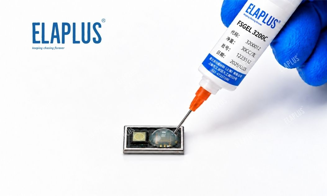
Inside a complete pressure sensor, it is possible to use FSGEL 3200C together with another peripheral potting / sealing material.
Example: MEMS chip zone → low-stress gel protection Peripheral PCB or cavity → insulating potting Housing seam → structural sealing PIN pins → interface sealing
This is zoned packaging, instead of using one single adhesive for the whole sensor.
XIV. 5 Questions NOT Recommended When Sourcing MEMS Packaging Materials
| Common Question | Better Question to Ask |
|---|---|
| What is the hardness of this adhesive? | How to verify the stress exerted on chips after curing? |
| Is it waterproof? | What media will it contact in service? |
| What is its temperature resistance? | Working temperature and peak temperature respectively? |
| Can it fill the whole cavity? | Which zones truly need protection? |
| Do you have MEMS-specific adhesive? | What are the failure risks of my MEMS structure? |
Proper material selection does not start by fixing the model number first. It starts with identifying failure risks, then matching materials.
FAQ|Common Questions on MEMS Low-Stress Packaging
Q1: Why do MEMS pressure sensors require low-stress materials? A: MEMS works relying on tiny mechanical deformation. Excessive packaging stress may change the stress state of sensitive structures.
Q2: Can ordinary epoxy potting be directly used for MEMS? A: It cannot be generalized. If high-modulus epoxy is applied directly on sensitive chip cores, curing shrinkage, zero point and thermal drift must be fully verified.
Q3: What is the biggest difference between fluorosilicone gel and ordinary silicone? A: Both can form flexible protection. But when exposed to oil, fuel vapor and certain complex chemical media, fluorosilicone systems are preferred for medium resistance evaluation.
Q4: Can FSGEL 3200C fully fill pressure sensors? A: Full filling depends on the structure. For MEMS applications, its primary value is local flexible protection on sensitive regions; full bulk filling is not recommended blindly.
Q5: Can soft gel protect gold wires? A: It does not lock gold wires like rigid resin. Instead, it forms a flexible buffering and environmental isolation layer around gold wires and solder joints.
Q6: What to do if zero drift occurs after MEMS potting? A: Compare zero-point data before dispensing, after curing, under high/low temperature and after thermal cycling. Check gel volume, coverage area and curing conditions.
Q7: Can FSGEL 3200C be used for magnetic steel bonding? A: Not suitable. Magnetic steel requires structural bonding; high-strength structural adhesives should be selected.
Q8: How to confirm the selected MEMS protective adhesive is correct? A: Final validation cannot rely only on adhesive properties. The packaged MEMS zero point, sensitivity, thermal drift, medium aging and long-term reliability must meet design specifications.