For temporary masking of selected local pads, metallic contact areas or other designated surfaces prior to plating, pickling and surface finishing of PCBs, ELAPLUS UV 1036 peelable UV-curable acrylic adhesive may be evaluated. Key validation shall cover coating resistance to process media, edge protection integrity, curing state and peel residue after treatment. In precision electronics manufacturing, temporary masking materials serve to shield regions excluded from processing and shall be removed as required upon process completion; they are not intended for long‑term structural bonding or permanent insulation.
Plating, pickling, sandblasting, spraying and other surface treatment steps in electronic manufacturing often demand selective protection of partial areas. Conventional options include masking tapes, films, fixtures and other dedicated protective materials, yet conforming around intricate geometries and irregular components can prove challenging.
Peelable UV adhesives form temporary protective layers via dispensed deposition and cure under specified ultraviolet irradiation. They offer a candidate process for small, irregularly shaped zones or applications requiring automated dispensing.
1. Why Peelability Alone Is Insufficient for Temporary Masking
A qualified temporary masking solution must satisfy requirements across three phases: protection, processing and removal. Loss of coating integrity during surface treatment may lead to unintended etching or deposition on protected regions.
Insufficient adhesion of the cured coating may trigger premature delamination under liquid flushing or mechanical handling. Conversely, overly strong bonding or locally thin coatings can cause tearing, residue or substrate damage during final peeling.
Accordingly, material selection for temporary masking cannot rely merely on initial tack or cure speed. Process chemistry, coating geometry and peeling method must all be incorporated into the design.
2. Key Requirements for Different Surface Treatment Processes
| Process Scenario | Primary Risks | Core Masking Requirements | Validation Focus |
|---|---|---|---|
| Selective Plating | Penetration of plating solution, edge deposition | Continuous edge profile, chemical compatibility | Mask boundary and peel performance |
| Pickling | Attack by chemical media | Stable resistance and adhesion under immersion | Post‑soak appearance |
| Sandblasting / Shot Peening | Mechanical impact and abrasion | Retention of coating integrity | Mask performance after impact |
| Spray Masking | Overspray onto non‑target areas | Sharp, well‑defined mask edges | Surface condition after peel |
| Local Machining Protection | Friction, chips and coolant exposure | Resistance to mechanical and chemical attack | Integrity after machining |
| Local PCB Protection | Complex boundaries around pads and devices | Controlled dispensing and removability | Residue and electrical performance |
Note that UV 1036 shall not be deployed across all above processes without prior qualification. Applications involving strong acids, strong alkalis, high‑temperature plating and severe mechanical impact require separate testing; peelability alone does not guarantee suitability.
3. Material Characteristics of UV 1036 for Evaluation
ELAPLUS UV 1036 is a one‑component UV‑curing acrylic adhesive, ranging in appearance from transparent to pale yellow. It features rapid UV cure and retains a degree of flexibility after cross‑linking, making it a candidate for temporary fixturing and surface protection of electronic components.
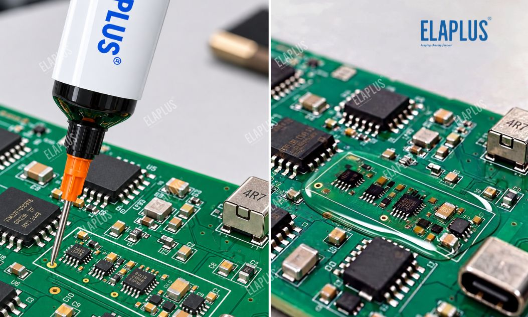
For designated PCB components, partial pads or metallic surfaces, an automated dispensing process can be assessed to form continuous masking films removable as an intact layer once processing concludes.
Successful full peeling depends on coating thickness, substrate adhesion, cure completeness and actual process exposure. Special attention is required for rough, porous or stepped geometries, where adhesive wicking into micro‑crevices may hinder clean removal.
UV 1036 is not intended for unvalidated high‑temperature or heavily corrosive workflows. Its published temperature rating does not equate to long‑term stability in all chemical environments.
4. Selection among Temporary Masking Adhesives, Tapes and Custom Fixtures
| Masking Method | Advantages | Principal Limitations | Suitable Applications |
|---|---|---|---|
| UV 1036 Peelable Adhesive | Point dispensing, adaptable to complex contours | Requires cure and peel validation | Irregular local masking |
| Masking Tape | Simple workflow, easy replacement | Poor conformability on intricate edges | Flat, regular areas |
| Pre‑formed Masking Film | Consistent patterning for repeated runs | Demanding positioning and geometry constraints | High‑volume regular structures |
| Mechanical Masking Fixture | Reusable | High upfront tooling cost and sealing boundary risks | High‑repeatability stations |
| Other Media‑Resistant Protective Materials | Formulated for specialised chemistries | Potentially complex removal procedure | Specialised surface finishing |
Masking tapes or fixtures often deliver superior cost efficiency for large, regular flat zones. UV 1036 merits priority assessment where numerous small, irregular local regions require protection and high dispensing throughput is desired.
ELAPLUS: Match adhesives to working conditions, rather than overemphasising nominal parameters. The essence of temporary masking is not maximising bond strength, but maintaining intact protection throughout processing and enabling reliable removal afterwards.
5. Why Mask Edges Matter More Than Central Zones
During surface treatment, process media tend to migrate along coating edges, substrate steps or local gaps into protected areas. Even if the central portion of a mask remains intact, discontinuities at edges can compromise the whole protection scheme.
For PCB pads and miniature electronic components, dispensing paths shall cover the intended protected footprint and yield continuous, controllable bead profiles along perimeters. For designs requiring intact peeling, adhesive ingress into deep, undercut or inaccessible recesses shall be avoided.
For larger temporary masks, tailored coating profiles can improve peelability, provided edge geometry does not encroach upon the required protected area.
6. Control of Automated Dispensing and UV Curing for UV 1036
Prior to dispensing, inspect PCBs, metal substrates or other target surfaces to eliminate oil contamination and particulate matter that may impair adhesion. Define dispensing trajectories, shot volumes and coating thickness according to the geometry of zones to be masked.
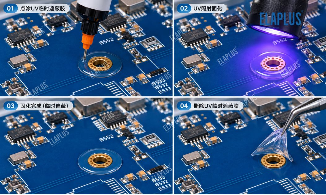
During automated dispensing, prevent adhesive wicking into unintended connectors, moving assemblies and narrow deep gaps. Continuous masking regions may be laid over multiple adjacent small components where specified, without impairing neighbouring functional devices.
For UV curing, verify wavelength, radiant energy, working distance and shadowed areas against material specifications. Freedom from surface tack alone does not confirm full cure through the masking layer; sidewalls of components and shaded regions require separate inspection.
Once cured, examine mask edges and overall integrity before commencing formal surface treatment. Processes involving elevated temperature, aggressive chemicals or mechanical impact shall first pass coupon qualification before a mass‑production process window is locked in.
7. Practices to Avoid Residue after Processing
Removal of temporary masking adhesive shall follow a peeling strategy optimised for the substrate and coating structure. Continuous peeling motion is preferred; sharp tools capable of scratching metallic plating or PCB surfaces shall be avoided.
Recurring tearing at fixed locations typically points to insufficient local thickness, problematic step geometry or incomplete curing. Random residue indicates inconsistent coating, surface contamination or incompatibility with process fluids.
For plated contact pads or metallic surfaces scheduled for subsequent soldering, visual inspection and functional testing shall confirm no residual contamination interfering with downstream operations.
8. Adaptation for Different Manufacturing Scenarios
For protection of local PCB pads, tight control over adhesive boundaries, UV curing and post‑peel solderability is essential. For selective masking on metallic parts prior to plating, validation shall focus on plating bath compatibility, edge penetration and surface condition after removal.
For pickling or polishing of precision components, testing shall replicate actual acid composition, abrasive media and mechanical loading. For spray applications, interaction between the masking coating and topcoat materials must be checked to ensure peeling does not damage the finished layer.
Identical cure and peel parameters cannot be reused across disparate processes; independent process windows shall be established based on the production BOM and operating conditions.
FAQ
Q: Can UV temporary masking adhesive be used before selective PCB plating?
A: UV 1036 may be evaluated, subject to validation of plating solution compatibility and mask edge integrity.
Q: Can fully cured UV 1036 be peeled off directly?
A: It is formulated for peelable applications, yet clean removal depends on substrate, coating thickness, cure state and process exposure.
Q: Is temporary masking adhesive suitable for pickling?
A: Suitability must be validated against actual acid composition, concentration, temperature and dwell time; universal compatibility cannot be assumed.
Q: Is a thicker masking layer always better?
A: Not necessarily. Excessive thickness complicates curing and peeling, while insufficient thickness risks protection failure.
Q: Can UV masking adhesive replace permanent conformal coating?
A: No. Temporary masking is designed for process shielding and subsequent removal, with a fundamentally different function from long‑term conformal protection.